
Interconnects, the wires that string transistors together into circuits on microchips, have long been built from copper due to its high conductivity. However, as electronics continue to shrink, copper becomes a dramatically worse conductor. Now scientists find that a new class of materials containing exotic quasiparticles might one day help enable next-generation interconnects that become better conductors the thinner they get.
The problem that copper interconnects now face has to do with the mean free path of the metal, the average distance an electron can travel before it runs into a molecule. Once copper wires shrink beneath this limit—in copper’s case, 40 nanometers—their electrical conductivity drops dramatically because their electrons start experiencing more collisions.
Researchers are investigating other metals that show better conductivity at nanometer scales for use in interconnect. For instance, cobalt and ruthenium have electron mean free paths of 10 nm and 6 nm, respectively. This means interconnects made from these metals can get smaller than copper wires before running into the same conductivity problem. However, if they shrink far enough, they will have to deal with the same challenge.
In a new study, scientists instead investigated topological materials, which possess extraordinary properties based on the topology of their structures. The researchers synthesized nanowires made of one such material as a proof of concept.
“We do not need super-pristine or high-quality samples or super-low temperatures or high vacuum to see the quantum effects,” says Judy Cha, a professor of materials science and engineering at Cornell University. “Our measurements were done at room temperature in low vacuum or in air. This to me is astonishing.”
Why topology could uncover next-gen interconnects
Topology is the branch of mathematics that investigates what aspects of shapes can survive deformation. For instance, an object shaped like a doughnut can get deformed into the shape of a mug, with the doughnut’s hole forming the hole in the cup’s handle, but it could not get pushed or pulled into a shape that lacked a hole without ripping the item apart.
Employing insights from topology, researchers first developed a kind of topological material called an electronic topological insulator in 2007. Electrons zipping along the edges or surfaces of these materials are “topologically protected” from the kind of scattering observed in standard conductors, meaning they strongly resist any disturbances that might hamper their flow, much as a doughnut might resist any change that would remove its hole.
However, while topological insulators are conductive on their surfaces, they remain insulating in their bulk. In contrast, different topological materials known as Weyl semimetals both are conductive in their bulk and possess topologically protected conductive states on their surfaces. This makes them “much more conducting than topological insulators,” says Cha.
Weyl semimetals get their special conductive properties from quasiparticle versions of Weyl fermions, theoretical subatomic particles that are massless and carry electric charge. (Quasiparticles are collective excitations of atoms within materials that behave as if they are particles in free space.)
These quasiparticles make the surfaces of Weyl semimetals more conductive. So, as wires of Weyl semimetals get thinner, and the ratio between their surface and their volume increases, the surface contribution to electrical conduction should also grow. This could theoretically give them an advantage over other materials in interconnects as they shrink.
Niobium arsenide nanowires show promise
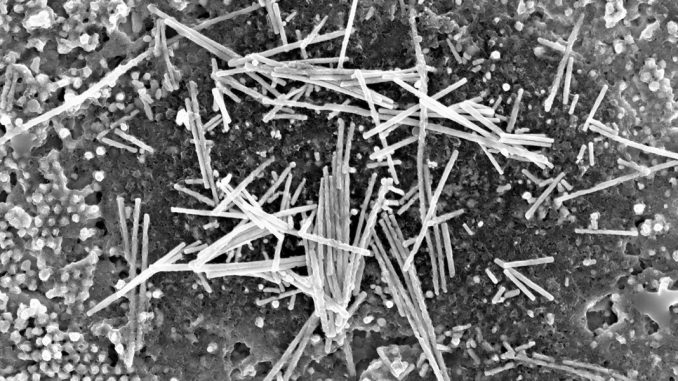
In the new study, Cha and her colleagues synthesized nanowires of the Weyl semimetal niobium arsenide using a method known as thermomechanical nanomolding. This method allowed the researchers to make a single-crystal nanowire two to three micrometers long and as thin as 40 nanometers wide.
The scientists found the resistivity of niobium arsenide nanowires dropped with decreasing diameter. At room temperature, a 40-nm-wide nanowire displayed a resistivity about 70 percent lower than that of bulk single crystals. Their analyses suggest this improvement was due to surface conduction.
Although the 40-nm-wide niobium arsenide wires were more conductive than the same size cobalt or ruthenium wires, they did not prove more conductive than state-of-the-art 10-nm-thick copper interconnects. However, the researchers expect niobium arsenide nanowires about 12 nm in diameter to outperform such copper interconnects. At roughly that diameter or less, the surface contribution of these nanowires to their electrical conduction will exceed the bulk contribution, they say.
In addition, the nanowires proved stable in air and could safely carry a high amount of electrical current before they broke down. They also showed high thermal conductivity, which could help them prevent overheating if they were to serve as interconnects.
However, Cha notes that niobium arsenide may ultimately not prove a practical replacement for copper. “Arsenic is toxic,” she notes. In addition, the synthesis technique they used is not compatible with CMOS or industry back-end-of-line processing conditions.
Still, Cha says their proof-of-principle work shows Weyl semimetals may display a key advantage over conventional materials when it comes to scaling down, and that even imperfect nanowires of Weyl semimetals with many defects can show enhanced conduction. “Topological semimetals are compelling and realistic engineering materials for applications, rather than remaining as model systems for physicists in academia,” Cha says.
Topological semimetals besides niobium arsenide may also be promising. For instance, in June at the IEEE/JSAP VLSI Symposium, Samsung presented research on molybdenum phosphide, and IBM presented work on cobalt monosilicide. “Industry is paying attention,” Cha says.
The scientists detailed their findings online 16 July in the journal Science.
From Your Site Articles
Related Articles Around the Web



