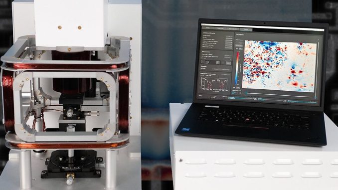
Chipmakers are increasingly stacking transistor-packed layers on top of each other to cram even more computing power into any given space. However, today’s technologies for spotting buried defects that can ruin these 3-D chips are either inadequate or downright destructive. But, new quantum sensors based on artificial diamonds might help foundries quickly catch these hidden defects during production without damaging chips, possibly saving billions of dollars, a startup says.
Defects that arise with regards to the interconnects through which current flows in a microchip, “whether they come from metal not deposited right, or a crack in the silicon, or whatever, will lead to that chip not working, and so you have to throw it away,” says Sanjive Agarwala, co-founder and CEO of quantum technology company EuQlid in College Park, Maryland. “And with the rise of 3-D sandwich integration, with stacks of layers of silicon, you have to throw out the entire sandwich. That’s a massive, massive problem.”
Mostly “the way industry deals with this problem today is by passing the costs down to the end user,” Agarwala says. “If we can help solve this problem, we can help bring prices down, bring revenue up, and more and more markets can take advantage of these capabilities.”
Currently, the main way the semiconductor industry spots potential defects is with optical techniques to visually detect problems, Agarwala says. But that technology faces real challenges when it comes to peering into thick stacks. “We need new 3-D inspection techniques to see problems during manufacturing.”
Although X-ray inspection can see defects within vertical stacks, it works relatively slowly, “and X-rays damage silicon,” Agarwala says. “No one uses X-ray inspection during manufacturing—it’s primarily used for failure analysis.”
Quantum sensors from artificial diamonds
EuQlid‘s claims its quantum sensor platform, QuMRI, can quickly find defects in 3D stacks by precisely mapping how current flows in deeply buried interconnects and do so in a non-destructive, contactless manner, Agarwala says. “We’re 100 times faster than X-ray, and we don’t damage what we image,” he notes.
Quantum sensors take the biggest challenge for quantum computers—unwanted interference, or noise—and transform it into a strength. Noise disrupts quantum computers because the quantum effects they use for computation are extraordinarily vulnerable to outside interference. But quantum sensors depend on those disturbances to detect minuscule changes in, say, magnetic and electric fields.
At the heart of the quantum sensors in QuMRI are microscopic artificial diamonds. Each has a defect within them, in which a carbon atom is replaced with a nitrogen atom and the adjacent carbon atom is missing. When these nitrogen-vacancy (NV) centers are illuminated with green light, they fluoresce red. Magnetic disturbances from nearby electric currents alter this response, allowing NV centers to serve as sensors.
Agarwala says QuMRI can achieve similar precision to X-ray inspection to depths of 100 to 150 micrometers, “which for the foreseeable future is what the semiconductor industry needs.”
In a statement, Paul van der Heide, materials and component analysis director at leading semiconductor research center Imec, says “EuQlid’s Qu-MRI addresses a foundational technology need for the design and manufacturing of next-generation semiconductors, by non-invasively visualizing buried connectivity defects.”
Beyond spotting buried defects, potential applications for QuMRI includes protection against cybersecurity vulnerabilities called hardware trojans. “Let’s say I hide a Trojan in a chip that can send information about what that chip is doing,” Agarwala says. “When it’s running, it can create current flow, and we’ll be able to detect the Trojan.”
From Your Site Articles
Related Articles Around the Web


Be the first to comment